- 您现在的位置:买卖IC网 > Sheet目录2003 > LTC1408IUH#TRPBF (Linear Technology)IC ADC 14BIT 600KSPS 32-QFN
9
LTC1408
1408fa
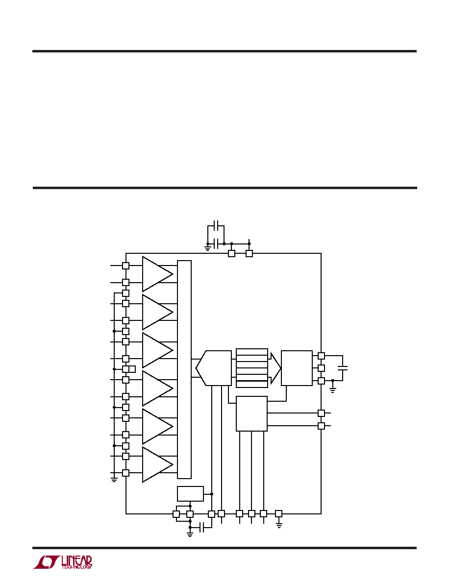
BLOCK DIAGRA
W
2
OGND
1
SD0
3
OVDD
3V
–
+
4
5
24
23
S & H
–
+
7
6
9
12 13
16
19
8
S & H
GND
EXPOSED PAD
VREF
10
F
CH0–
CH0+
CH1–
CH1+
–
+
10
11
S & H
–
+
14
15
S & H
CH2–
CH2+
CH3–
CH3+
–
+
17
18
S & H
–
+
20
21
S & H
CH4–
CH4+
CH5–
CH5+
10
F
0.1
F
LTC1408
DGND
32
SCK
30
CONV
SEL2 SEL1 SEL0
THREE-
STATE
SERIAL
OUTPUT
PORT
MUX
2.5V
REFERENCE
TIMING
LOGIC
VCC
25
3V
VDD
1408 BD
600ksps
14-BIT ADC
14-BIT LATCH 5
14-BIT LATCH 4
14-BIT LATCH 3
14-BIT LATCH 2
14-BIT LATCH 1
14-BIT LATCH 0
26
27
BIP
29
28
31
22
33
0.1
F
CONV (Pin 30): Convert Start. Holds the six analog input
signals and starts the conversion on the rising edge. Two
pulses with SCK in fixed high or fixed low state starts Nap
mode. Four or more pulses with SCK in fixed high or fixed
low state starts Sleep mode.
DGND (Pin 31): Digital Ground. This ground pin must be
tied directly to the solid ground plane. Digital input signal
currents flow through this pin.
SCK (Pin 32): External Clock Input. Advances the conver-
sion process and sequences the output data at SD0 (Pin1)
on the rising edge. One or more pulses wake from sleep
or nap power saving modes. 16 clock cycles are needed
for each of the channels that are activated by SELx (Pins
26, 27, 28), up to a total of 96 clock cycles needed to
convert and read out all 6 channels.
EXPOSED PAD (Pin 33): GND. Must be tied directly to the
solid ground plane.
UU
U
PI FU CTIO S
发布紧急采购,3分钟左右您将得到回复。
相关PDF资料
LTC1409IG#TR
IC ADC 12BIT 800KSPS SMPL 28SSOP
LTC1410IG#TR
IC ADC 12BIT 1.25MSPS SMP 28SSOP
LTC1411IG#TRPBF
IC A/D CONV 14BIT 2.5MSPS 36SSOP
LTC1412IG#TR
IC ADC 12BIT 3MSPS SAMPLE 28SSOP
LTC1414IGN#TRPBF
IC A/D CONV 14BIT SAMPLNG 28SSOP
LTC1415CG#TRPBF
IC A/D CONV 12BIT SAMPLNG 28SSOP
LTC1416IG#TR
IC ADC 14BIT 400KSPS SMPL 28SSOP
LTC1417AIGN#TR
IC ADC 14BIT 400KSPS SMPL 16SSOP
相关代理商/技术参数
LTC1408IUH-12#PBF
功能描述:IC ADC 12BIT 600KSPS 32-QFN RoHS:是 类别:集成电路 (IC) >> 数据采集 - 模数转换器 系列:- 其它有关文件:TSA1204 View All Specifications 标准包装:1 系列:- 位数:12 采样率(每秒):20M 数据接口:并联 转换器数目:2 功率耗散(最大):155mW 电压电源:模拟和数字 工作温度:-40°C ~ 85°C 安装类型:表面贴装 封装/外壳:48-TQFP 供应商设备封装:48-TQFP(7x7) 包装:Digi-Reel® 输入数目和类型:4 个单端,单极;2 个差分,单极 产品目录页面:1156 (CN2011-ZH PDF) 其它名称:497-5435-6
LTC1408IUH-12#TRPBF
功能描述:IC ADC 12BIT 600KSPS 32-QFN RoHS:是 类别:集成电路 (IC) >> 数据采集 - 模数转换器 系列:- 标准包装:1,000 系列:- 位数:16 采样率(每秒):45k 数据接口:串行 转换器数目:2 功率耗散(最大):315mW 电压电源:模拟和数字 工作温度:0°C ~ 70°C 安装类型:表面贴装 封装/外壳:28-SOIC(0.295",7.50mm 宽) 供应商设备封装:28-SOIC W 包装:带卷 (TR) 输入数目和类型:2 个单端,单极
LTC1409CG
功能描述:IC A/D CONV 12BIT SAMPLNG 28SSOP RoHS:否 类别:集成电路 (IC) >> 数据采集 - 模数转换器 系列:- 标准包装:1,000 系列:- 位数:12 采样率(每秒):300k 数据接口:并联 转换器数目:1 功率耗散(最大):75mW 电压电源:单电源 工作温度:0°C ~ 70°C 安装类型:表面贴装 封装/外壳:24-SOIC(0.295",7.50mm 宽) 供应商设备封装:24-SOIC 包装:带卷 (TR) 输入数目和类型:1 个单端,单极;1 个单端,双极
LTC1409CG#PBF
功能描述:IC A/D CONV 12BIT SAMPLNG 28SSOP RoHS:是 类别:集成电路 (IC) >> 数据采集 - 模数转换器 系列:- 标准包装:1,000 系列:- 位数:12 采样率(每秒):300k 数据接口:并联 转换器数目:1 功率耗散(最大):75mW 电压电源:单电源 工作温度:0°C ~ 70°C 安装类型:表面贴装 封装/外壳:24-SOIC(0.295",7.50mm 宽) 供应商设备封装:24-SOIC 包装:带卷 (TR) 输入数目和类型:1 个单端,单极;1 个单端,双极
LTC1409CG#TR
功能描述:IC ADC 12BIT 800KSPS SMPL 28SSOP RoHS:否 类别:集成电路 (IC) >> 数据采集 - 模数转换器 系列:- 标准包装:1,000 系列:- 位数:12 采样率(每秒):300k 数据接口:并联 转换器数目:1 功率耗散(最大):75mW 电压电源:单电源 工作温度:0°C ~ 70°C 安装类型:表面贴装 封装/外壳:24-SOIC(0.295",7.50mm 宽) 供应商设备封装:24-SOIC 包装:带卷 (TR) 输入数目和类型:1 个单端,单极;1 个单端,双极
LTC1409CG#TRPBF
功能描述:IC A/D CONV 12BIT SAMPLNG 28SSOP RoHS:是 类别:集成电路 (IC) >> 数据采集 - 模数转换器 系列:- 标准包装:1,000 系列:- 位数:12 采样率(每秒):300k 数据接口:并联 转换器数目:1 功率耗散(最大):75mW 电压电源:单电源 工作温度:0°C ~ 70°C 安装类型:表面贴装 封装/外壳:24-SOIC(0.295",7.50mm 宽) 供应商设备封装:24-SOIC 包装:带卷 (TR) 输入数目和类型:1 个单端,单极;1 个单端,双极
LTC1409CSW
功能描述:IC A/D CONV 12BIT SAMPLNG 28SOIC RoHS:否 类别:集成电路 (IC) >> 数据采集 - 模数转换器 系列:- 标准包装:1,000 系列:- 位数:12 采样率(每秒):300k 数据接口:并联 转换器数目:1 功率耗散(最大):75mW 电压电源:单电源 工作温度:0°C ~ 70°C 安装类型:表面贴装 封装/外壳:24-SOIC(0.295",7.50mm 宽) 供应商设备封装:24-SOIC 包装:带卷 (TR) 输入数目和类型:1 个单端,单极;1 个单端,双极
LTC1409CSW#PBF
功能描述:IC A/D CONV 12BIT SAMPLNG 28SOIC RoHS:是 类别:集成电路 (IC) >> 数据采集 - 模数转换器 系列:- 标准包装:1,000 系列:- 位数:12 采样率(每秒):300k 数据接口:并联 转换器数目:1 功率耗散(最大):75mW 电压电源:单电源 工作温度:0°C ~ 70°C 安装类型:表面贴装 封装/外壳:24-SOIC(0.295",7.50mm 宽) 供应商设备封装:24-SOIC 包装:带卷 (TR) 输入数目和类型:1 个单端,单极;1 个单端,双极